Introduction
Polycrystalline CVD diamond, sintered from countless tiny diamond microcrystals, features a hardness close to natural diamond, and thermal conductivity 4 to 5 times higher than pure copper, making it the top-tier thermal management material widely applied in high-power semiconductors, infrared optical windows, 5G RF devices and aerospace thermal control systems.
However, as-grown CVD diamond plates are generally thick and come with inherent thickness inconsistency, which cannot meet the strict requirement for uniform thin wafers in chip bonding and high-precision heat sink packaging processes. Precision thinning of polycrystalline diamond has long been a universal, high-difficulty bottleneck that the entire global advanced material processing industry has been struggling to solve.
Verified 4-Inch CVD Diamond Thinning Case
Project Specifications
| Item |
Detailed Parameters |
| Processing Material |
4-inch polycrystalline CVD diamond, initial thickness 1mm |
| Core Processing Requirement |
Uniform full-wafer thinning from 1mm down to 0.5mm |
| Adopted Equipment |
Sanyi Laser Dedicated Polycrystalline Diamond Laser Grinding System |
Core Processing Challenges Faced

The project requires full-wafer uniform removal of 500μm material, which means half of the original 1mm thick diamond wafer needs to be removed evenly across the entire 100mm 4-inch surface. Processing on the hardest known engineering material with such massive removal amount brings 5 irreplaceable pain points that traditional mechanical grinding cannot resolve:
- Extreme Material Hardness: CVD diamond reaches Mohs hardness level 10, far higher than any common grinding wheel material
- Massive Uniform Removal Requirement: 500μm full-wafer consistent removal cannot be achieved via low-efficiency polishing processes for mass production
- Ultra-Strict Large-Area Uniformity Control: Any minor inconsistency during the thinning process will amplify the Total Thickness Variation (TTV), directly leading to failure in subsequent wafer-level bonding procedures
- High Stress Fracture Risk for Thin Wafers: Traditional mechanical grinding applies heavy contact pressure on workpieces. For large-area thin diamond wafers with pre-existing residual stress and warpage from the CVD growth process, it is extremely easy to cause edge chipping, full-wafer crack and even total fracture
- Hidden Sub-Surface Damage: Traditional mechanical grinding will generate microcracks and dislocation layers extending deep into the diamond wafer, which will permanently degrade the core thermal conductivity and optical performance of the finished wafer
Core Advantages of Sanyi Laser Non-Contact Thinning Technology
Sanyi Laser's dedicated polycrystalline diamond laser grinding process completely replaces traditional mechanical contact processing, directly solves the long-standing "low processing speed, high brittleness breakage loss, high consumable cost" pain points in the industry:
✅ Non-contact processing, zero mechanical stress applied on the wafer. There is no grinding pressure throughout the full processing cycle, which fundamentally eliminates the risk of edge chipping and full-wafer fracture for large-size thin diamond wafers, pushing finished product yield to a new high level
✅ Fully digitally controllable thickness. Powered by Sanyi Laser's self-developed dedicated motion control software, all process parameters are precisely regulated. The system automatically runs layered scanning following the pre-set target thickness, ensuring consistent removal depth and fully controllable TTV, completely getting rid of the manual experience dependent "thickness inconsistency by feel" problem in traditional processing
✅ Highly controllable thermal impact. With ultra-precise laser energy regulation, the process effectively suppresses unnecessary diamond graphitization and thermal stress induced micro-cracks
✅ Full large-size compatibility. The system supports full processing coverage for polycrystalline diamond wafers ranging from 1 inch to 8 inches, matching all mainstream specifications in power semiconductor and optical application scenarios
✅ Top-tier processing quality. The system stably controls wafer TTV and warpage at the micron level, and the finished surface roughness reaches sub-micron level without extra polishing procedures
Final Verified Processing Results
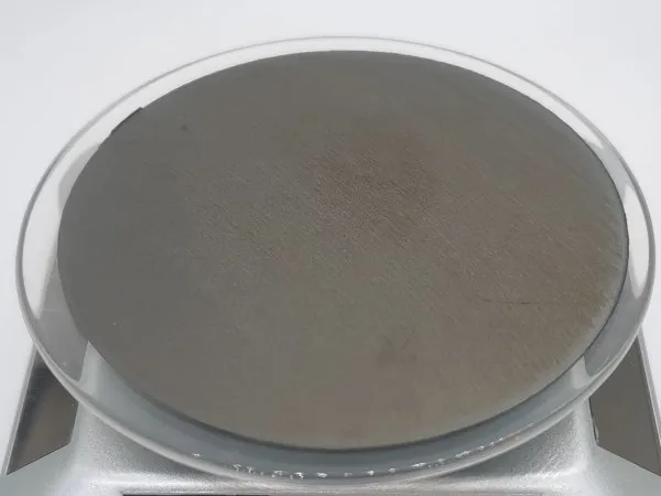
After being processed by the Sanyi Laser polycrystalline diamond laser grinding equipment, the 4-inch polycrystalline CVD diamond wafer of our customer was evenly thinned from the initial 1.0mm to the target 0.5mm, achieving stable 500μm uniform single-side removal:
- Excellent full-wafer thickness uniformity, the Total Thickness Variation (TTV) across the whole wafer is strictly controlled at the micron level, completely eliminating local over-grinding or under-grinding defects caused by uneven pressure in traditional mechanical grinding
- No mechanical indentation damage on the thinned surface, no large-area graphitized black edge defects
- The wafer edge is perfectly intact, with zero chipping and zero through-cracks
- The overall wafer warpage is extremely low, fully meeting all strict requirements for subsequent chip bonding, heat sink packaging and optical processing of the customer
Product Value for Mass Production Deployment
The Sanyi Laser polycrystalline diamond laser grinding system is purpose-built to overcome the precision thinning bottleneck for ultra-hard thin wafers. Replacing traditional mechanical grinding with non-contact laser processing, it fundamentally solves the industry-wide pain points for large-size diamond thinning, including easy edge chipping, high fracture rate, uncontrollable TTV and high grinding wheel consumable cost.
Equipped with in-house developed laser control software and high-precision motion platform, the system achieves fully uniform thickness removal via digital layered control. The equipment supports processing for 1 to 8 inch polycrystalline diamond wafers, and is configured with multi-position fixtures to enable continuous batch processing, pushing overall processing efficiency up by an order of magnitude, while completely eliminating mechanical stress induced damage and delivering remarkable yield improvement.