Products
Diamond Laser Equipment
Cold Laser Diamond Cutting Machine
Green Laser Diamond Cutting Machine
Infrared Laser Diamond Cutting Machine
4P Green Laser Diamond Cutting Machine
PDC Laser Engraving Machine
Cold Laser Diamond Marking Machine
7D Fancy Cut and Engrave Laser Diamond Machine
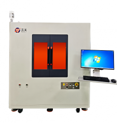
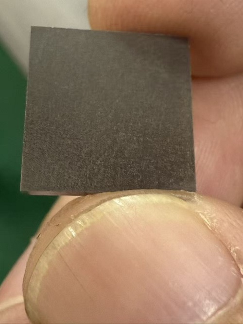
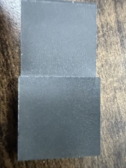
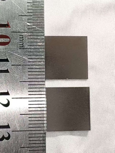
PDC Sheet Laser Cutting and Drilling Machine
Doped Diamond Laser Cutting and Drilling Machine
Diamond Wire-Drawing Dies Laser Drilling Machine